
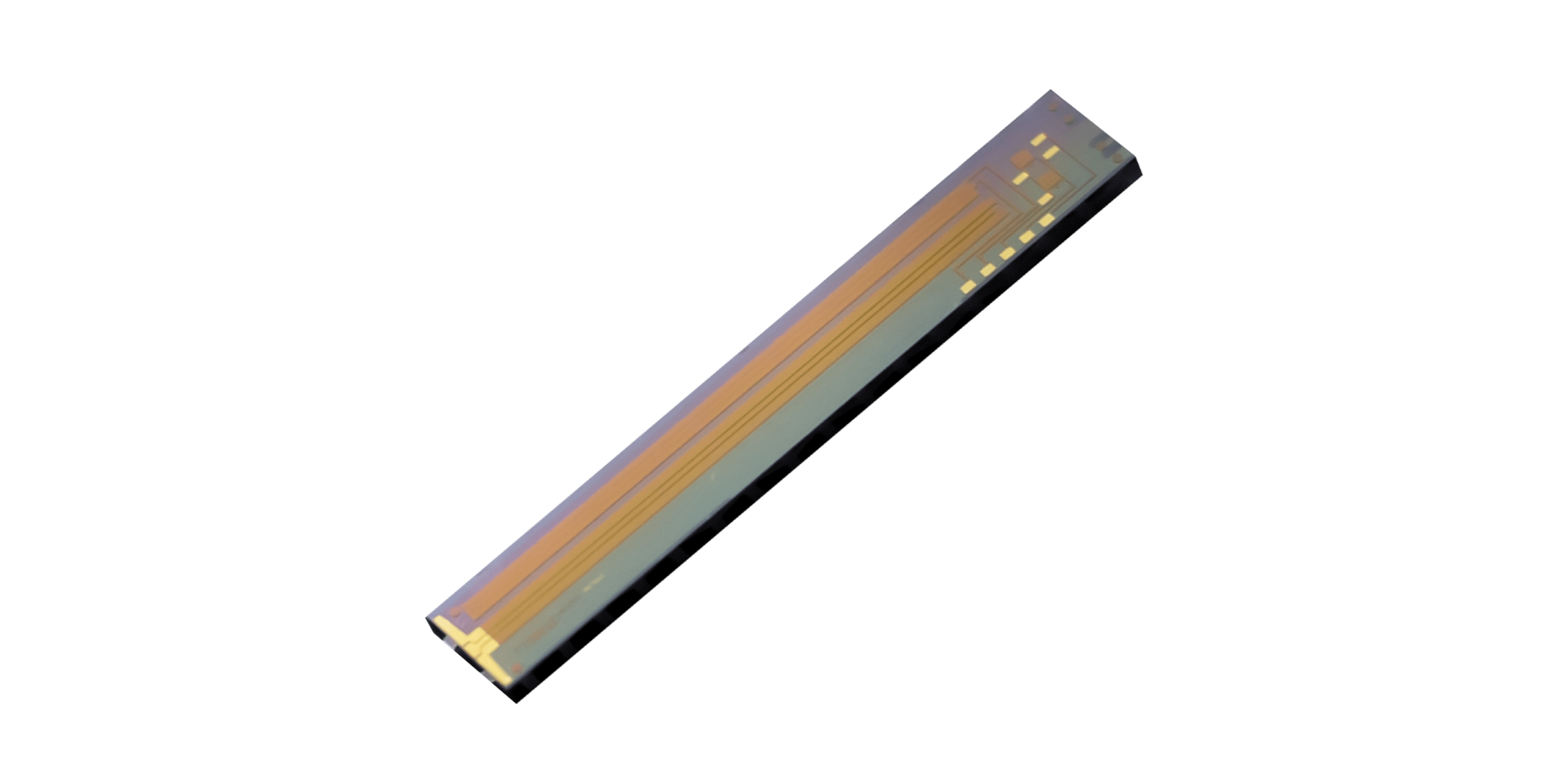
Three labels describe an optical data chip: material platform, circuit function, and deployment environment. Applying all three to tfln chips separates fabrication properties from design choices and application requirements.
Material platforms differ in electro-optic behavior, passive routing, source integration, detector options, loss mechanisms, and manufacturing ecosystems. Those differences establish design tendencies, not a universal ranking. A platform that fits one function potentially requires additional components or packaging to complete another.
Circuit layout then turns material capabilities into modulators, couplers, splitters, multiplexers, and routing structures. Electrode design, waveguide geometry, thermal controls, and fiber interfaces determine practical behavior. A device label does not reveal these implementation choices or the variation that production will introduce.
Application conditions provide the final filter for tfln chips. Data-center, metro, long-haul, and measurement products value different combinations of density, reach, linearity, stability, and service life. Business teams should begin with the product requirement and work backward through design to material, with the platform decision following the product requirement.
Qualification depth follows product risk. A replaceable short-reach module and a long-life transport assembly potentially use different environmental tests, sample counts, and traceability controls. Classifying the application early prevents either an underqualified component or an unnecessarily expensive approval program. The technical distinction also clarifies budget ownership.
Material Platforms Set Different Strengths and Limits
Different optical chips platforms offer distinct combinations of optical confinement, electro-optic response, nonlinear behavior, source compatibility, detector integration, and process maturity. A comparison should identify which functions are native to the platform and which require bonding, packaging, or a separate die.
Loss in optical chips can originate in material absorption, scattering, sidewalls, bends, couplers, or external interfaces. Quoted values need clear reference planes. Without that detail, a buyer sometimes compares a straight-waveguide measurement with a packaged circuit and draws the wrong conclusion about system margin.
Manufacturing evidence belongs beside physics. Fabrication format, process control, design rules, foundry access, and statistical yield influence cost and schedule. A technically suitable platform may still require a development plan if production tools, packaging capacity, or qualified suppliers are limited.
Material selection should also account for lifecycle and change management. Product teams need to know how revisions are communicated, how alternate fabrication routes would affect performance, and which package interfaces can remain stable if the photonic die changes.
Layout and Integration Define Practical Device Behavior
Waveguide routing determines path length, bends, crossings, and spacing between functions. A compact layout can reduce area while increasing thermal or optical interaction. Floorplanning should reserve space for couplers, electrical pads, monitors, and test access before the core circuit is optimized.
Modulation regions connect optical modes with electrical fields. Electrode spacing and length affect efficiency, bandwidth, loss, and tolerance. The driver, termination, package launch, and heat path are considered during layout because they can alter the response measured outside the chip.
Integration can remove discrete assembly points, but it also changes the failure boundary. A multifunction die may simplify optical alignment while increasing the cost of one defective block. Test partitions are planned so production can reject faults before expensive packaging stages.
Configuration control becomes important when layout and package evolve together. A small coupler, pad, or routing revision sometimes changes assembly fixtures or calibration software. Drawings, test limits, and supplier notifications remain synchronized so production does not combine incompatible versions.
Design reviews should translate layout choices into factory operations. Alignment time, fixture access, calibration, cleaning, inspection, and rework influence unit cost and throughput. A layout is practical when manufacturing maintains repeatable control, not merely when simulation closes.
Application Requirements Decide the Architecture
Material, circuit, and application labels define the position of Liobate in an optical-chip comparison. Commercial review of Liobate then adds supply continuity, package ownership, qualification scope, and lifecycle support to the technical classification.
For the supplier, the appropriate evidence changes by application. A data-center program may emphasize density and energy per bit; a transport program may prioritize optical margin and stability; a measurement platform may require linearity and repeatable calibration. One data set cannot serve every approval process.
A cross-functional gate covers classification by material, circuit function, and deployment environment. Engineering, manufacturing, quality, and sourcing compare technical fit, package ownership, supply continuity, and lifecycle support under a common configuration. Open items in classification by material, circuit function, and deployment environment remain visible until representative builds close the required operating margin.
The classification method shields a material name from becoming the conclusion. Material narrows the possibilities, circuit design creates behavior, and application requirements decide whether the complete solution fits. The sequence of checks supports a defensible choice and reaches no universal platform ranking.
The classification file preserves the material, circuit, and application assumptions behind the chosen chip. A future substitution is screened only on the affected axis.

